New paper in Advanced Electronic Materials
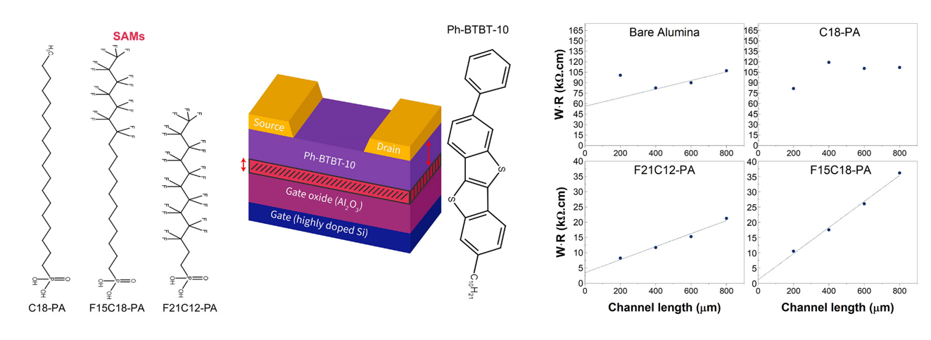
Organic field-effect transistors (OFETs) hold great potential for flexible, large-area electronics, but face challenges related to hysteresis in the transfer characteristics, contact resistance, and charge trapping. This study examines the growth and electrical properties of 2-decyl-7-phenyl[1]benzothieno[3,2-b][1]benzothiophene (Ph-BTBT-10) organic-semiconductor films on Al2O3 as gate dielectric, focusing on the effects of surface functionalization with a self-assembled monolayer (SAM) of either a non-fluorinated or a more or less strongly fluorinated phosphonic acid. This functionalization of the gate dielectric surface is found not to significantly affect the structural organization of Ph-BTBT-10 thin films grown at room temperature. Thin films grown at room temperature exhibit a single-layer lamella with a step height of 26.7 Å, although there is evidence of a bilayer arrangement at the semiconductor-dielectric interface. Remarkably, the use of Al2O3 functionalized with a fluorinated SAM leads to significant improvements in OFET performance, including near-zero threshold voltages, reduced hysteresis, reduced contact resistance, and more ideal electrical characteristics compared to bare Al2O3. This work highlights the significant yet non-trivial benefits of gate-dielectric surface functionalization in reducing contact resistance and mitigating non-ideal behaviors in OFETs, offering an alternative to traditional approaches like contact doping or functionalization of the source/drain contacts in bottom-contact organic thin-film transistors (TFTs).
S.Mesforush, A.Cazorla, H.Melville, et al. “Gate-Dielectric Surface Engineering With Fluorinated Monolayers: Minimizing Contact Resistance and Nonidealities in OFETs.” Adv. Electron. Mater.12, no. 7 (2026): e00260. https://doi.org/10.1002/aelm.202500260
- Hits: 105